PCB Board Design: STM32 USB Dongle with Accelerometer
In this project, I designed a 4-layer printed circuit board (PCB) using Altium Designer, following a comprehensive YouTube tutorial to understand best practices in schematic creation, layout, and design for manufacture. The project involved creating a USB dongle featuring an STM32 microcontroller and an MPU-6050 accelerometer.
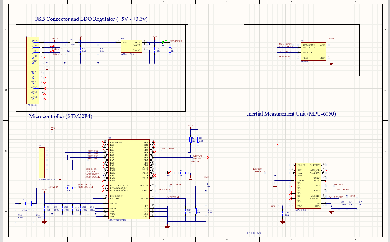
Schematic Design
I began by designing the schematic in Altium using available component libraries. Key features and design considerations included:
- Decoupling and filtering: Low-pass capacitor filters were added to power lines, and ferrite beads were used where necessary to suppress high-frequency noise.
- Logic level management: Pull-up and pull-down resistors were implemented to ensure known states at GPIOs.
- Net organization: Effective net labeling and grouping were used to ensure clarity during the PCB layout phase.
- USB interface integration: A USB Type-A connector was added, with the corresponding data lines routed to the STM32’s USB peripheral pins.
To correctly assign STM32 pins, I used STM32CubeIDE to generate the pinout based on peripheral requirements and validated the connections. I then ran an electrical rules check (ERC) in Altium to ensure no floating nets, short circuits, or unconnected pins were present before moving to PCB layout.
PCB Layout and Design
After schematic validation, I transitioned to designing the physical PCB:
- 4-layer board stackup: The design used a 4-layer configuration to simplify trace routing and improve EMI performance. Layers were organized as:
- Top Layer: Signal
- Inner Layer 1: Ground Plane
- Inner Layer 2: Power Plane
- Bottom Layer: Signal
- Component placement: Components were strategically placed to minimize trace lengths, reduce interference, and ensure a compact layout. High-priority components (e.g. the STM32 and MPU-6050) were placed close together, especially those interacting directly with high-speed signals like USB.
- Routing considerations:
- Power traces were widened where necessary and tapered as they approached destination pins to manage space without compromising performance.
- Since high current was not involved, 90-degree angles were acceptable in traces.
- Vias were used extensively to transition between layers, especially when routing signals under components or to avoid conflicts.
Manufacturing Preparation
To finalize the design:
- Tooling and mounting holes were added for enclosure compatibility and ease of assembly.
- Manufacturer guidelines (JLCPCB in this case) were consulted to adhere to trace width, clearance, and via size minimums.
- Gerber files, drill files, and a Bill of Materials (BOM) were generated and exported from Altium.
- The project files were uploaded to JLCPCB for fabrication and assembly.
Key Skills Gained:
- Proficiency in Altium Designer for schematic capture and PCB layout
- Understanding of PCB manufacturing constraints and stackup planning
- Applying embedded hardware design principles, including decoupling, filtering, and pinout planning
- Experience preparing Gerber and BOM files for real-world PCB production
- Basic use of STM32CubeIDE for peripheral and pin configuration
This project provided a solid foundation in PCB design, from concept to production, and offered a hands-on understanding of how embedded systems are physically realized.
Below is an image of the schematic for the USB dongle.